DipTrace Free 2.2.0.0
interface. DipTrace Free has many features, such as: PCB Layout with powerful autorouter, Schematic Capture, Pattern Editor, Component Editor. DipTrace is the most userfriendly software for PCB Designers.
Rip-up-and-retry autorouter and flexible manual routing tools allows you to route single- and multilayer PCB’s quickly and efficiently. The accurate shape based copper pour system supports 5 types of filling and different thermals. The DRC function allows you to check the clearance between design objects, minimum size of tracks, and drills, errors are displayed graphically and you can fix them step-by-step and rerun the DRC in one click after any corrections. Output formats are DXF, Gerber and N/C Drill.
Special Edge exporting function allows you to produce the PCB’s using milling machine (DXF to G-code converter required). Standard libraries contain 40.000+ components. Freeware Edition has “250 pins, 2 signal layers” limit and manufacturing output disabled, other features including printing are the same as Full Edition.
Easy to learn user interface:
· To design a schematic, simply select and place components onto your document and connect them together using the wire and bus tools. Multisheet design is supported. Then select the menu option ‘Switch to Board’ to convert the schematic to PCB. Layout can be updated from Schematic in a few clicks at anytime. When you create or edit design objects they are highlighted to improve your work. Step-by-step tutorial available from web-site guides you through the design process and allows to get started with ease.
Easy to use manual and powerful automatic routing:
· DipTrace PCB software includes an advanced automatic router that is able to route single-layer and multi-layer boards. It is available with a ‘rip-up and retry’ algorithm. Autorouter achieves high completion rates by going back and re-routing nets to make space for connections that could not be routed on a previous pass. Intelligent manual routing tools allow you to create and edit traces by 90, 45 degree or without any limitations. Through, blind or buried vias can be used in automatic and manual routing. Unlimited board size is supported.
Shape-based copper pour:
· Powerful copper pour system can help to reduce your manufacturing costs by minimizing the amount of etching solution required. To use it, all you have to do is insert a copper area on your board in the PCB Layout program and any pad or trace inside the selected area will be automatically surrounded with a gap of the desired size. Using copper pour you can also create planes and connect them to pads and vias (different thermal types are supported).
Advanced Verification Features:
· Schematic and PCB design modules have number of verification features that help control project accuracy on different design stages: The ERC function shows possible errors in Schematic pin connections using defined rules and allows you to correct errors step-by-step. DRC function checks the clearance between design objects, minimum size of traces, and drills. Errors are displayed graphically and you can fix them step-by-step and rerun the DRC in one click after any corrections. Net Connectivity Check verifies if all nets of PCB are electrically connected. This feature uses traces, copper pour filled area and shapes to control connectivity, then reports broken and merged nets with area details. Comparing to Schematic allows you to check if routed PCB is identical with Schematic.
Import/Export Features:
· Package modules allow you to exchange schematics, layouts and libraries with other EDA and CAD packages. DipTrace Schematic Capture and PCB Layout also support Accel, Allegro, Mentor, PADS, P-CAD, Protel and Tango netlist formats.
Manufacturing output formats:
· DipTrace provides support for a number of different manufacturing output formats. Using this PCB software you can produce N/C Drill files for numerically controlled (N.C.) drilling machines and RS-274X Gerber files for sending to board manufacturers. Vectorizing function allows to export true-type fonts and raster images. Also DipTrace supports DXF output.
Producing PCBs using milling method:
· DipTrace allows you to export edge polylines to DXF. The DXF files can be converted to G-code with Ace Converter (it’s free). Before edge exporting the DRC function of pcb layout program checks the design and shows possible problems if exist.
Standard component libraries:
· DipTrace package includes component and pattern libraries which contain 50.000+ components from different manufacturers.
Creation of your own libraries:
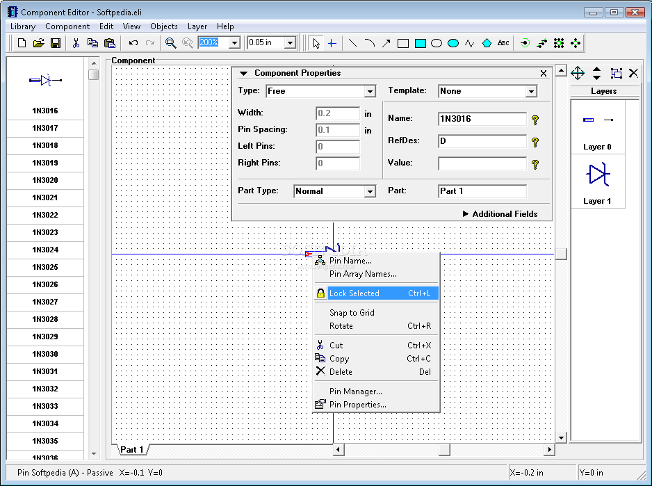
· Component and Pattern Editors allow to design your own symbols and patterns. To create complete components simply connect them together using Component Editor.
Limitations:
· 250 pins limit
· For non-profit use only
What’s New in This Release:
· 3D Preview in PCB Layout (.wrl and .3ds models are supported).
· 2580 3D models in .wrl format (separate download).
· Redesigned pattern and component libraries (full conformity).
· Strict Via Styles (changing via style changes all vias of the style).
· Net Classes (with extended rules). Class-to-Class rules.
· Improved DRC (more rules, separate rules by layers and net-classes, class-to-class rules). Show errors by layers or all. Show current clearance/size and necessary.
· All necessary dialog boxes and menus are redesigned to use net classes and via styles.
· Main menu redesigned (Layers item removed, sub-items moved to layers panel and Route menu).
· Inserting layers, moving layers up/down.
· Layer panel improved (buttons to add layer, layer setup and display mode; submenu; set current layer by double click)
· Layer Setup dialog box improved (insert layer, move up, move down).
Improved manual routing:
· 3 standard modes + custom mode;
· 7 possible segment configurations;
· fixed…
